
I am far enough into this project that I feel like I actually have interesting stuff to share. A while back I was starting to make serious plans to convert to a Megasquirt 3 Pro system, which included sketching out a very detailed wiring harness schematic since I wanted to add fully sequential injection, VW pencil coils, a hardwired MAF, knock sensing and wide-band O2 support using the factory harness. The desired features would require mods to the harness, and I wanted to have a complete sketch of the initial and final state of the wiring so that I could make it all factory-quality. Then I changed my mind and started working on a custom tune with Sssquid Tuning since that seemed like a faster way to get a tune dialed in which could be (sort of) transferred to MS3Pro later. Anyway, that was enough to get me started down the rabbit hole, so to speak, and I ended up starting to investigate stuff on a spare M1.7 ECU that I had laying around.
As you will see, it quickly spiraled out of control, down the rabbit hole I went, and I am fairly certain that nobody has ever seen this on here before. I found one other person on a Porsche forum who reverse engineered a 911 ECU PCB, but they posted a lot less information about their results. Since joining the E30 world 18 years ago, I remember seeing wacky threads like this where someone had way too much free time and did something interesting, and I always learned stuff and wished that I could someday do crazy projects. It looks like it is my turn.
If nothing else, this thread can be a reference for folks on the web who want to see how to DIY RE a multi-layer PCB with mostly-household tools and materials. This is still very much a work in progress, but the hardware parts of the RE effort are basically done. My attention is presently on the firmware and piecing together the last few details of the interface between some of the chips on the mainboard. My goals are as follows:
1) Build a complete schematic-driven PCB layout of all components and connections on the M1.7 mainboard - DONE!
2) Fill-in component values for resistors and capacitors, and characterize any Zener/Schottky/etc diodes - To Do (maybe)
3) Dump the total 40K of ROM (32K on the EPROM, 8K internal to the microcontroller) - DONE!
4) Disassemble the 40K ROM into assembly for understanding of its complete functionality - In progress
5) Rewrite the ROM code to make improvements to function (faster table lookup, wide-band O2 support, etc) - To Do pending #4
6) Other miscellaneous stuff I’ll mention when I get there
I am going to share the hardware aspects of this project since it is visually interesting and maybe people can learn some handy stuff which can help them repair their ageing ECU, or at least understand how it works a little better. It is really a fairly simple system compared to just about anything today, but it is very robust and it is more than capable of running a gasoline engine efficiently. You may be thinking "OK, fun times, but why the hell are you wasting so much time with this obsolete ECU when you could already be running MS3Pro?" That is a fair question. The answer is "why not?" Why bother owning and modifying a car as old as the E30 at all? Because...it is fun, you learn stuff and if you finally succeed you end up with something unique. Also, I am apparently incapable of going to sleep at a reasonable hour, regardless of what time I need to be up in the morning lol.
There is one thing that I am NOT going to do in here. That thing is posting map locations, types and how to edit them. The reason for this is that it is not my knowledge to give away. I worked with Sssquid Tuning on a custom tune for my 2.1L M42 last year, and in the process I started collaborating with him on some stuff. Unless he pops in here to detail how to DIY tune your own M1.x ECU (and I see no reason for him to do that), I am not going to post that stuff since I could not have figured it out without him.
OK, so that is a bit of an intro. Let's get into stuff that is a little more interesting. Images I post in here are very shrunken versions of the ones I have been working off of...I don't think that we need 500MB of pics in here lol. The stuff that follows is probably ~120 hours of work spread over the last year or so.
--------------------------------------------------------------------
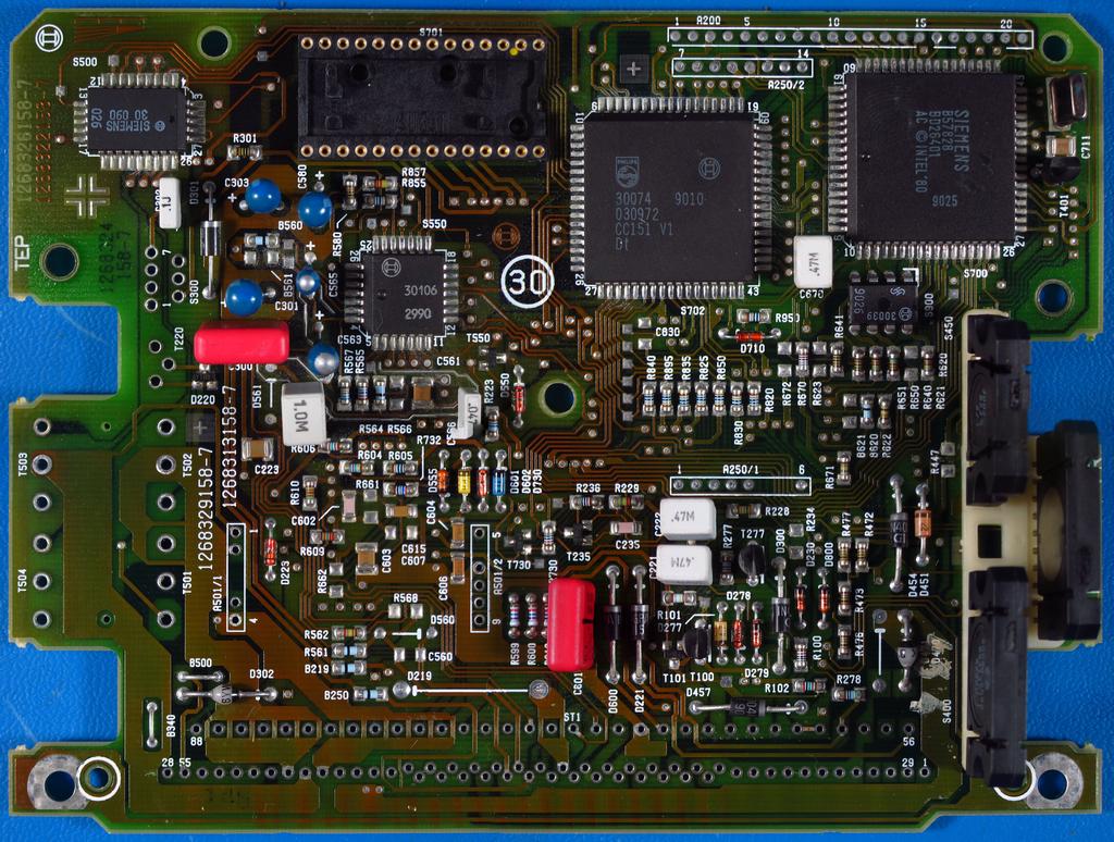
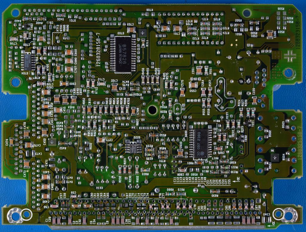
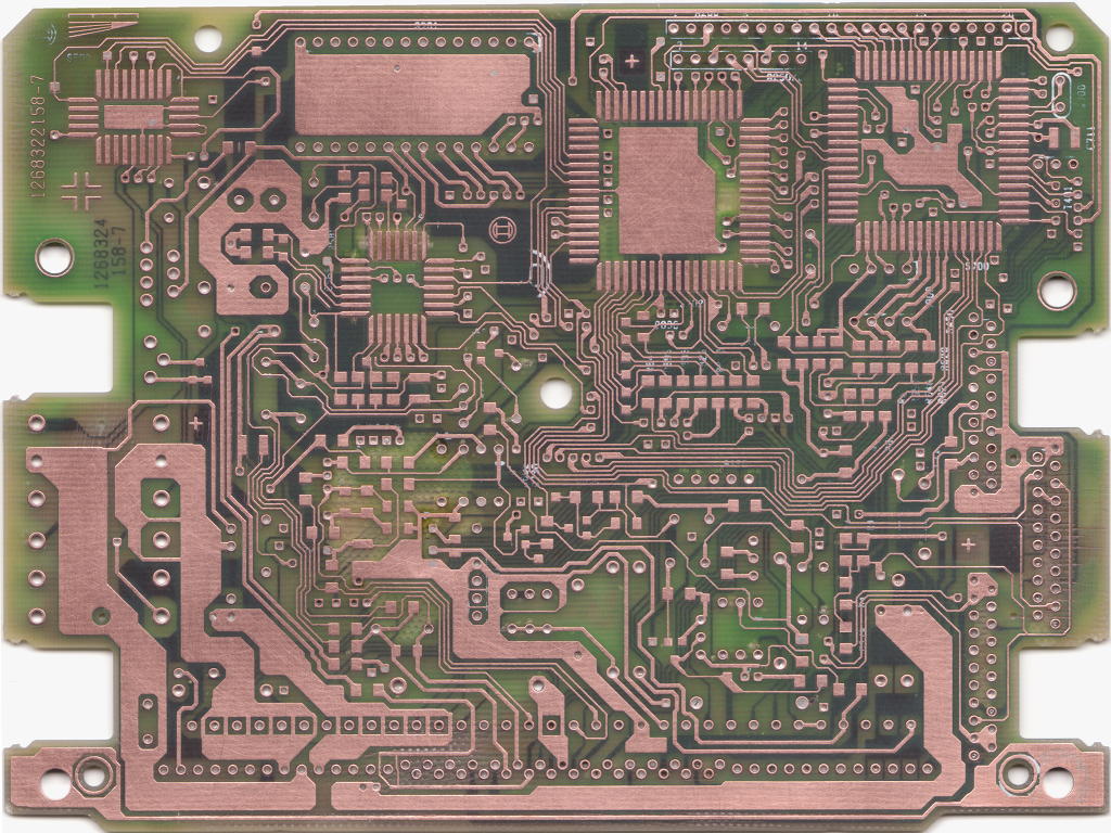
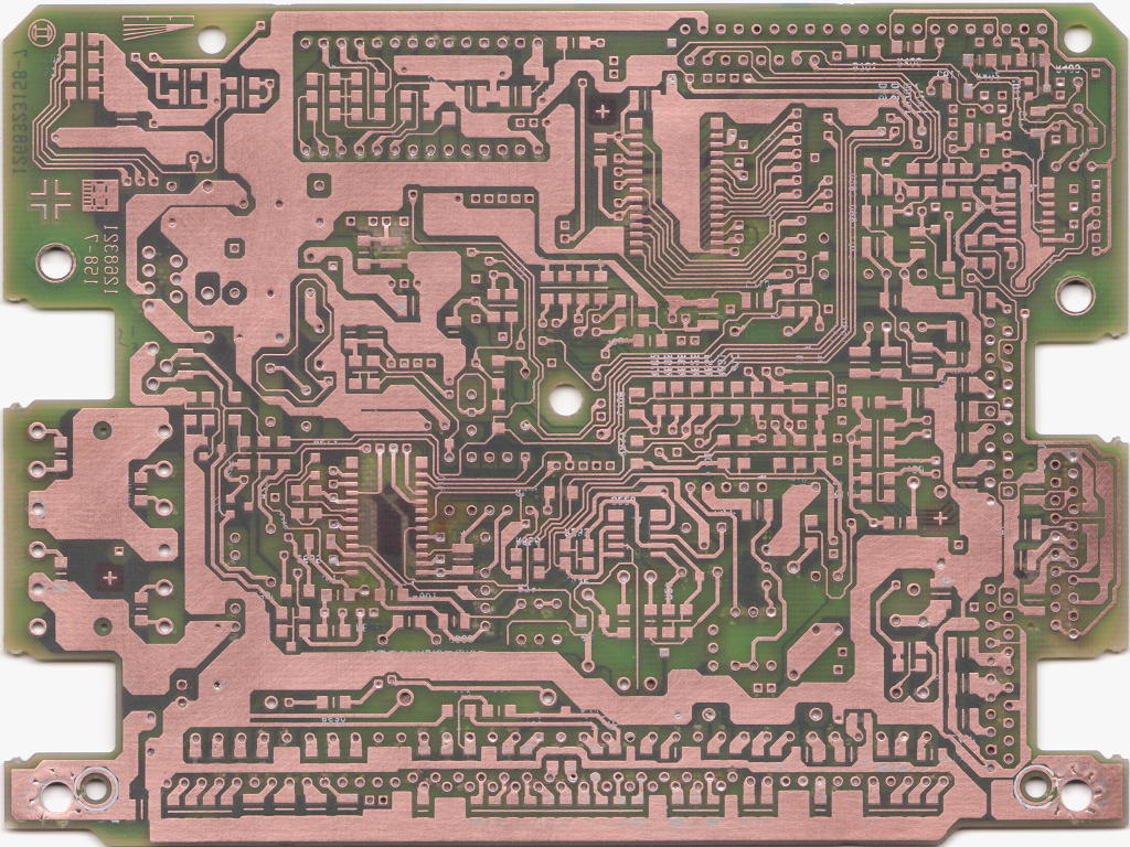
First, in order to understand the main PCB, I needed to build a schematic of the components on it. I started by getting detailed images of the populated top and bottom sides (a few of the larger components had been removed years ago). Each of these is actually 9 photos stitched together (the board was panned under a zoomed-in camera to get higher resolution).
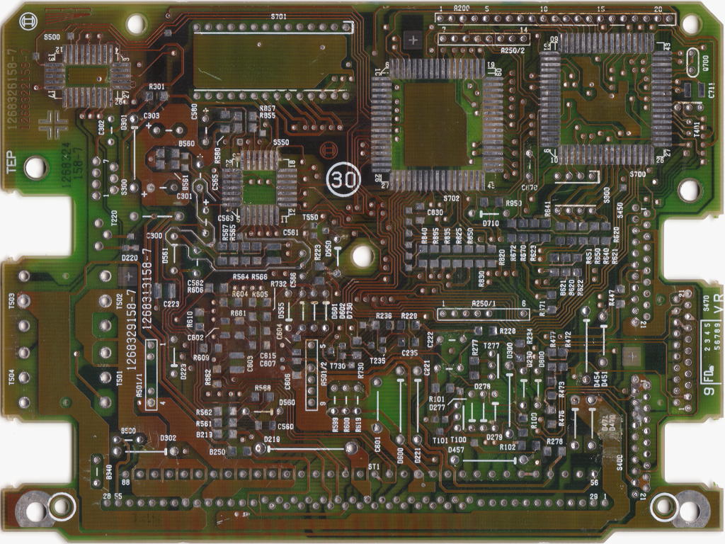
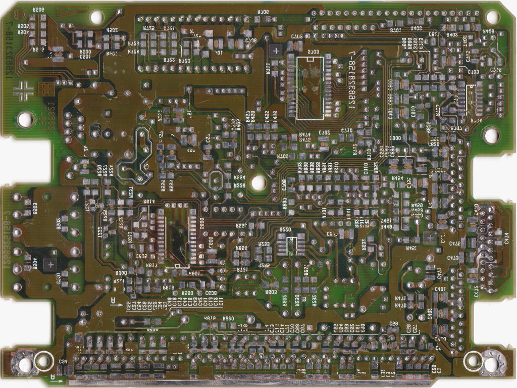
With that done, I depopulated the whole thing. Lots and lots of soldering iron action! I used a heat gun on some of the larger surface mount parts, which was sort of a mistake since the heat caused the internal layers to blister under the components. The problem with this arose later, which you will see. If I were to do it again, I would carefully use a Dremel and cut-off wheel to slice the leads at the plastic package and then remove the remaining leg pieces with the soldering iron. The PCB images hereafter were made with a flatbed scanner.
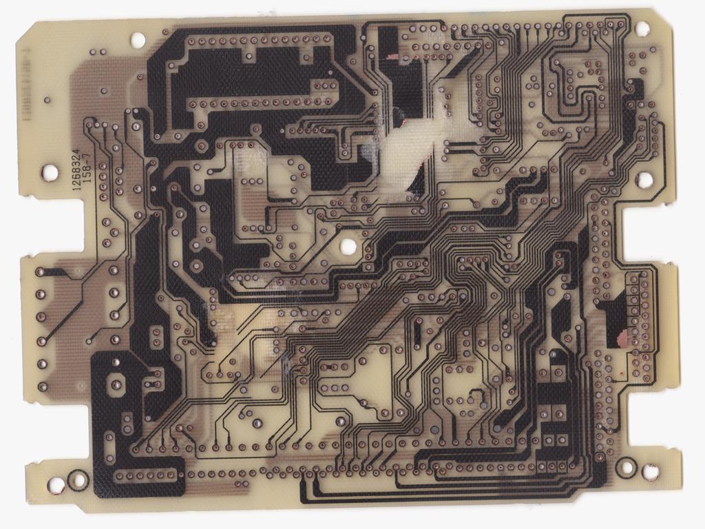
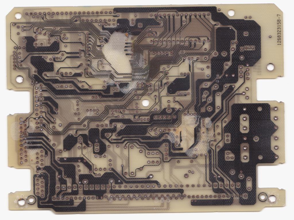
Next, the green solder mask layer was removed. I looked all over online for ways to do it chemically, but the chemicals required are a) not really accessible to hobbyists, and b) I don't need cancer. Instead, I got some 3M abrasive pads for metal polishing (they are a lot like the green scrubby pads you find everywhere, but more durable and finer) and attached them to a buffing attachment for my drill. This ended up wearing through a couple of small copper areas, but it was easy enough to reconstruct them in my image editor (GIMP). Again, layers were scanned.
That stuff was the easy part. This PCB had 4 layers, so seeing the outer ones was not going to be enough. Again, I scoured the web for ways to separate the layers, but there really was no good way of doing that. The main methods seemed to be to CNC the outer layers off, or spend hours and hours working with sandpaper. Since I have access to a manual mill at work, I used some double-sided tape to hold the PCB down and carefully removed the outer layers with a 20mm diameter end mill making ~0.25mm (~0.01”) deep passes. This worked surprisingly well.
As I had mentioned above, the layers blistered when I used a heat gun, and this caused some of the internal copper to be chopped off during milling.
It was no big deal. This is because copper cannot cross copper on a layer, so matching up what-went-where was pretty simple via deductive reasoning. Also, I could see "through" the outer layer scans enough to confirm things. There were no vias (inter-layer connecting holes) in these areas, which is why they blistered as badly as they did, but it also meant that traces went exactly where they look like they did. I reconstructed the damaged areas in GIMP and had nice complete pictures of the inner layers.
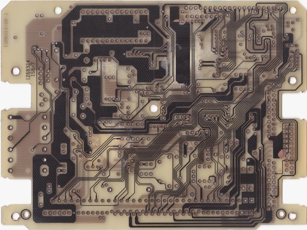
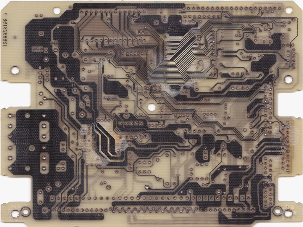
That was the easy part of it. I next needed to threshold the images to black/white so that I could use a free program (IMG2CAD) to convert them into DXF vector paths and import them into my schematic/layout program (DesignSpark PCB, free and very capable). There was a lot of manual touching-up to be done to get things to threshold properly, and I probably spent 6 hours tweaking the images in GIMP before vectorization. I also marked every single surface mount pad and plated through-hole so that those would be clear and obvious when I proceeded with future steps.
(layer 1 for example)
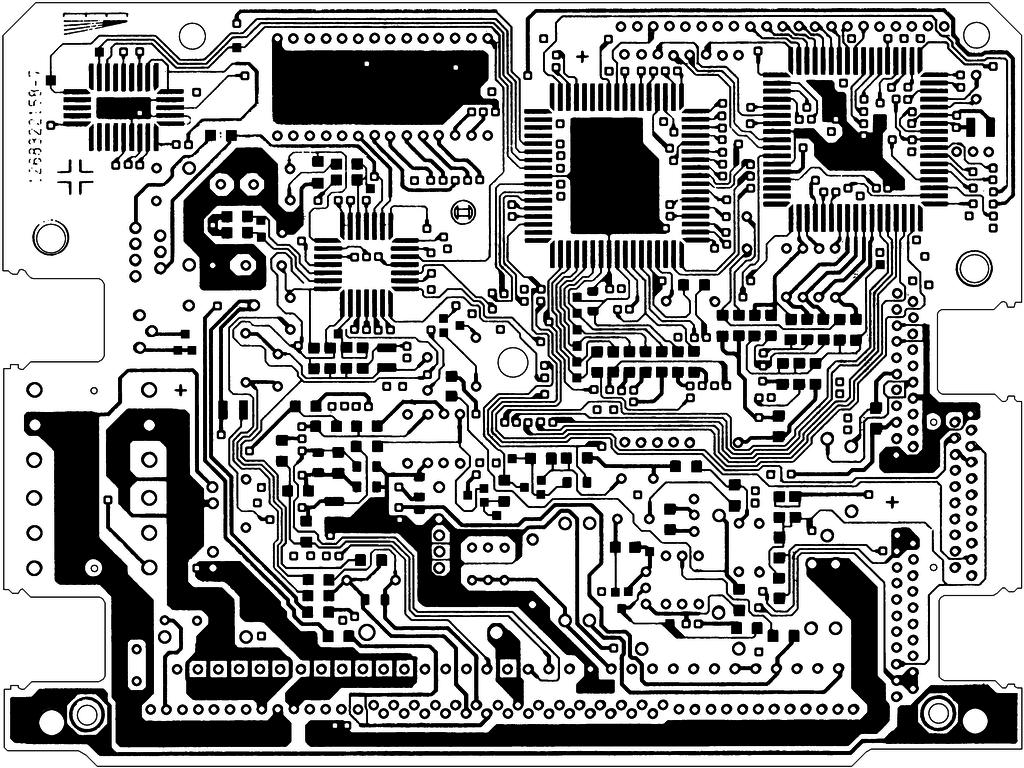
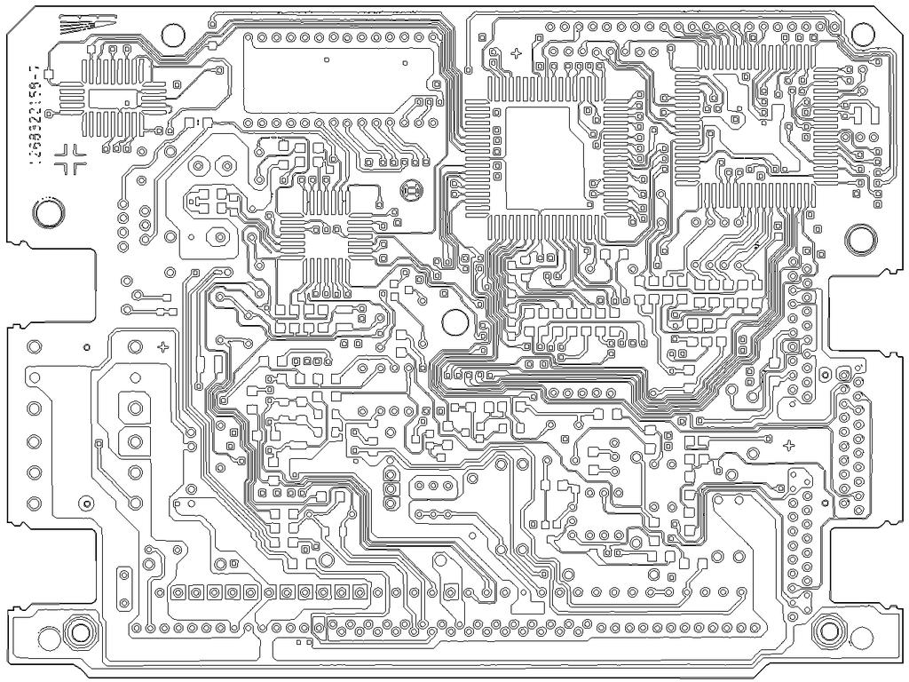
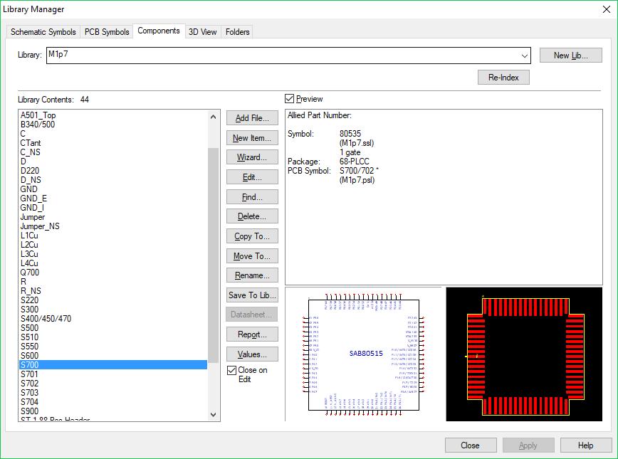
While I was marking pads and holes, I also noted dimensions of things. This was used to build a complete library of schematic symbols and components for the layout. Every single component was going to be accounted for in my reconstruction.
Here is where the real "fun" began. My intent was to have a schematic for the PCB so that it would be very easy to see what was what when I started messing with the firmware (which IO pin controlled what). Unfortunately, the standard for PCB layout programs is to start with a schematic and then drive the PCB components and netlist (terminal connections) from that...not the other way around. DesignSpark does allow you to create nets (connections) in the PCB manually, but it has no way of pushing them "backwards" into the schematic.
I almost gave up at this point. Building the schematic meant tracing all of the DXF geometry in the layout, exporting a text file which listed all of the PCB-only net names & connections, and then going into the schematic side and manually making matching connections & naming nets. Everything would have to be made exactly the same, manually. It was essentially like having to rebuild the circuit twice, one component and net at a time. Ultimately, I sucked it up and did it. It was not as bad as I thought it would be, and maybe 30 hours of work to do both workflows. Now I have a fully accurate PCB that is completely driven from the schematic, so when I do decide to make hardware mods to the mainboard, I can fully track and represent things.
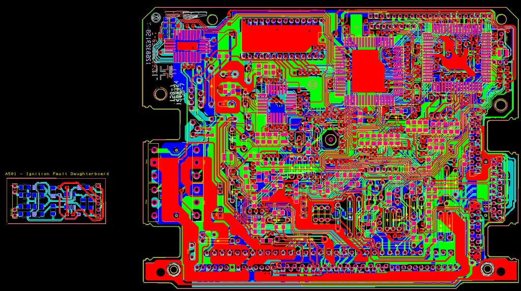
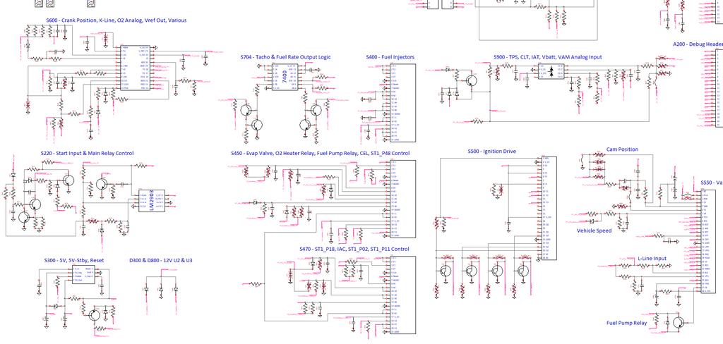
The PDF files in these links have the schematic and PCB artwork. The schematic is not well organized for viewing in a PDF since things are all separated out by subsystem with net labels indicting connections (a text search makes it easy to find endpoints though). This was to avoid having 200 crossed wires to wade through, since with the actual schematic in DesignSpark it is really easy to highlight nets and know what is connected where.
It is pretty interesting to see what was and was not populated on the board. These ECUs were used in all sorts of vehicles, and you can tell that the design was modular. Also, many of the pins on the main 88-position harness receptacle are connected to things on the PCB, but not used in the M42 wiring harness. Alfa Romeo used these on various 4 and 6 cylinder models, and the E36 M42 used M1.7.2 which is (as far as I can tell) the same main PCB but with the A250 daughter-board installed which processes knock sensor signals. I am actually planning to run my car on M1.7.2 once I get the firmware fully decoded so that I can eliminate E36-specific stuff like DISA control while also gaining knock sensing, but regular M1.7 is first since it will be 95% of the work needed anyway and my engine runs on it now.
There are a few partial schematics out on the web for other Motronic versions, and those were pretty helpful in figuring out what was what in my own ECU (meaning giving accurately descriptive names to nets). These included M1.3, M2.3.2 and M3.1. They all share enough in common with M1.7 to be super helpful. The M1.3 and M3.1 schematics are only partially complete and have a few errors in them, but I appreciate whoever it was that took the time to try to build them. The M2.3.2 one was posted on a different forum by a random member who was interested in RE'ing it, and it appears to be a 100% complete scan of an original (hand drawn!).
(Disclaimer)
None of these are mine, I did not make them and they were all found in various publicly-available parts of the internet where they were posted and/or created by others.
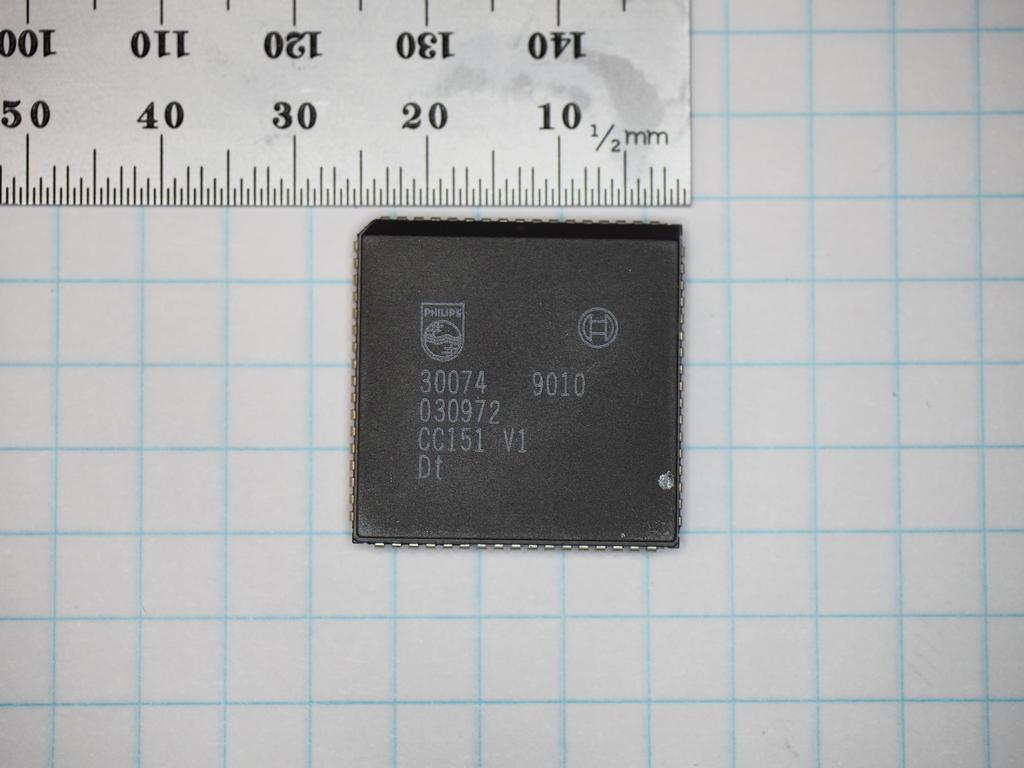
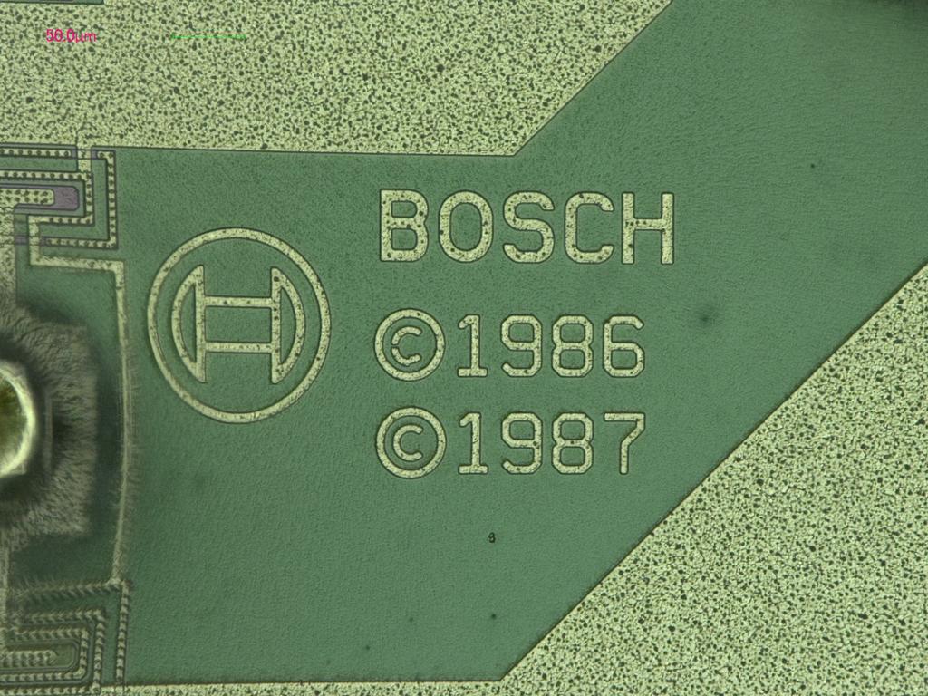
With that monster task out of the way, it was time to start digging in to the firmware. I have a program which disassembles 8051 microcode, so getting it into a rough representation of the assembly code was fairly easy. Separating out data constants from code is still a work in progress, as is determining what all of the RAM locations are storing and how chips like S500, S550 and S702 work. My main focus has been on S702 lately since it is critical to tons of functions. It is a port expander of some sort which seems to be a custom part made for Bosch to work with the main microcontroller. It is common to all three of the above listed Motronic versions, as well as mine, and I am sure it was used in others.
I have found how it is accessed in the firmware code and I understand a few of the instructions sent to it and how they control or read various pins. There is much more to it I think, like an internal timer/counter and other output functions which seem to be logical combinations of other input pins (such as pin 67 which seems to have its output programmed to be (A13 OR A14) OR (NOT A15)). I am not sure that I can figure this all out from the code, and since not all pins are even used in M1.7, I am going to need a lot more info on this thing if I want to use it to add functions.
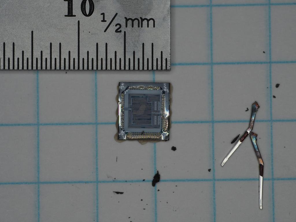
So, it was time to break in to S702 to start getting some idea of how it worked. "What?" Yes, literally breaking in to the chip to image the silicon die. I work in the electronics industry and my employer has some pretty high-end measurement equipment which they do not mind me using after-hours, so it's not really as silly as it sounds to literally look at the internal silicon. I had the S702 chip from the board I deconstructed above, so I just needed to get the epoxy encapsulation off. I wanted to do it chemically, but that involves sulfuric acid heated to 250 Celsius...no thanks. I found a method that just about anyone can use at home, and as crude as it is, it works.
I started with the chip and ground off the metal leads to get clean square sides.
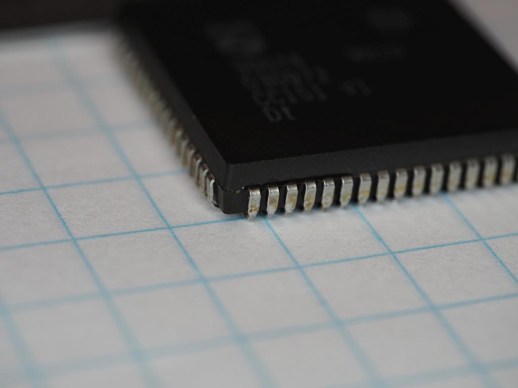
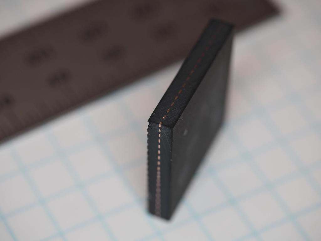
Then I stuck the chip in a cheapo bench vise, aligned the centerline with the top of the jaws and compressed it. I repeated this a few times, rotating the part, and it quickly popped apart.
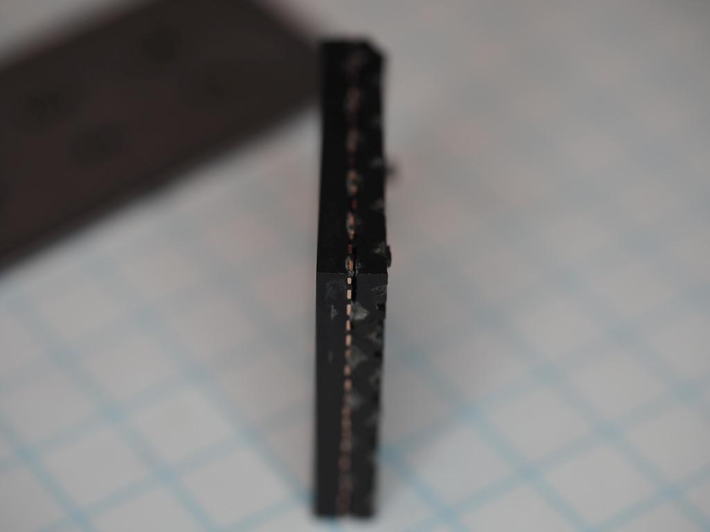
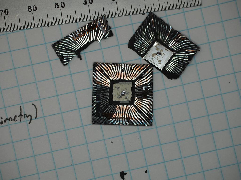
Voila, the actual functional bits of it. The actual "chip" is the little silicon die with all of the micro-features etched & plated onto it.
As I had said, I have access to various imaging equipment at work. Since the features on this are relatively large, an optical microscope was all that was needed to get a reasonable amount of detail from the die. The microscope I used does automatic 3D stitching, meaning I specify a 3D bounding box and it scans through all of the Z-heights, composites everything into perfect focus, pans to the next X/Y locations, repeats the Z steps and then stitches it all together into a big panorama with everything in focus. It is one of the lower magnification instruments in the lab since it only goes up to 2500X, but its automation functions make it one of my favorite instruments.
This chip was made with something around a 2 micron process (2000 nanometer, versus modern chips which are made with 10-30 nanometer processes). The link has a larger version, which is still a lot smaller than what I got out of the microscope, but more than enough for internet enjoyment. The distortion around the wire bonds is due to the fact that there is a clear adhesive encapsulation about 0.25mm thick covering the whole die. It was easy enough to see through, so I left it on.
300X mag die overview shot:
Full-size image (~8MB): http://www.e30tuner.com/assist/m17re...2_full300x.jpg
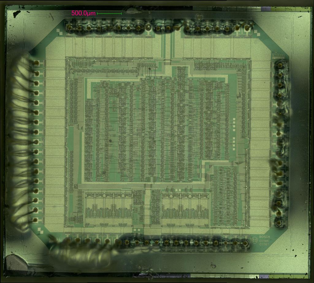
The smallest features/spacings were on the order of 1.5 microns. These images were taken at 500X to 2500X magnification.
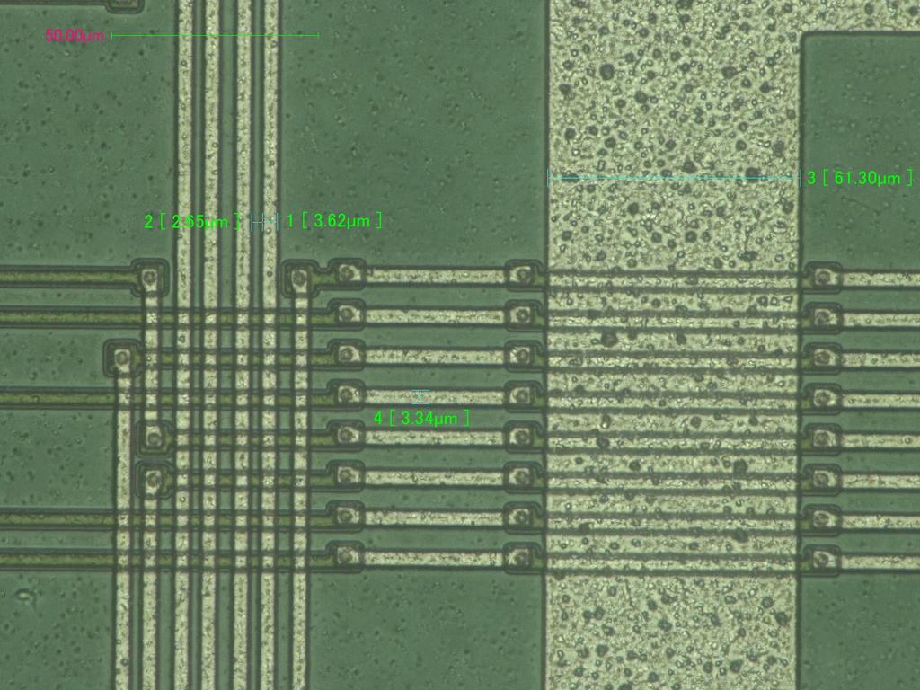
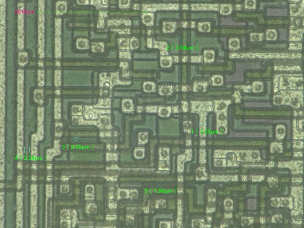
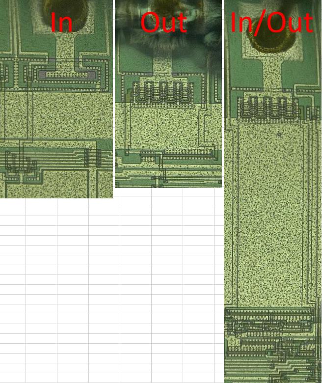
I am not about to go and try to trace out all of the individual transistors and logic gates since that is a lot of work, and it is probably faster to figure out what I need to know by messing with the firmware. But this was worth the effort since I was able to clearly identify three distinct pin types. Knowing which ones were inputs, outputs and bi-directional has been very helpful in understanding the command structure used to interface with it.
Inputs have a single metal trace coming from the wire pad, outputs have two and bi-directional ones have three.
For the time being, that is the high level recap of where I am at with this. I plan to break open the various other chips and image their dies too, just for fun. As crazy as the above stuff may or may not seem, it was actually all of 30 minutes worth of work thanks to the fancy microscope. If and when I come across other interesting stuff during my RE efforts, I will post the details. At one point I started a similar project on a cheap eBay M1.3 (from M20 cars), but it isn't really something I am all that interested in since I do not own an M20-powered car. The M1.3 PCB is only 2 layers and is somewhat less complex, although the core architecture is mostly the same as M1.7. When I am done with M1.7, I will be something like 90% of the way to doing the same thing to M1.3 since the hardware and firmware is actually very similar. But, don't hold your breath for that one!
Cheers everyone, I hope this is interesting for you!
--------------------------------------------------------------------
Unplanned philosophical mumbo-jumbo because I worked through a coupe of glasses of scotch while typing this up...
While there have been immense advances in semiconductor fabrication technology, chip design and our understanding of device physics since this chip was made, things have not actually changed at all in some respects. We can pack ~10000 more transistors into the same area now versus back then, but ultimately everything that goes on in all of our various devices which use silicon chips is just a bunch of transistors that form basic logical elements which take in and put out 1's and 0's (as high/low voltages). That's it, really. We just can't "see" it working in any literal way without working in the industry, so it seems like magic. That isn't to downplay the wild science and technology required to make this stuff work. The true bleeding-edge of applied human knowledge is found in the semiconductor world. It took all of human scientific knowledge from the beginning of our existence to make the first mass produced integrated circuit (lots of transistors on one silicon die) less than a century ago. With that, we were able to make better computers which were faster and smaller, with which we could design faster and smaller transistors, which made more powerful computers, which made more advanced transistors, etc. Hell, maybe transistors are the most advanced things on the planet, and we are their slaves. They are self-replicating and self-evolving, with us as their tools to do it. Hell, I exist because of the transistor! My parents both worked in the industry and that is where they met. Maybe that is a bit of a stretch...enough philosophy for now, I think.
As you will see, it quickly spiraled out of control, down the rabbit hole I went, and I am fairly certain that nobody has ever seen this on here before. I found one other person on a Porsche forum who reverse engineered a 911 ECU PCB, but they posted a lot less information about their results. Since joining the E30 world 18 years ago, I remember seeing wacky threads like this where someone had way too much free time and did something interesting, and I always learned stuff and wished that I could someday do crazy projects. It looks like it is my turn.
If nothing else, this thread can be a reference for folks on the web who want to see how to DIY RE a multi-layer PCB with mostly-household tools and materials. This is still very much a work in progress, but the hardware parts of the RE effort are basically done. My attention is presently on the firmware and piecing together the last few details of the interface between some of the chips on the mainboard. My goals are as follows:
1) Build a complete schematic-driven PCB layout of all components and connections on the M1.7 mainboard - DONE!
2) Fill-in component values for resistors and capacitors, and characterize any Zener/Schottky/etc diodes - To Do (maybe)
3) Dump the total 40K of ROM (32K on the EPROM, 8K internal to the microcontroller) - DONE!
4) Disassemble the 40K ROM into assembly for understanding of its complete functionality - In progress
5) Rewrite the ROM code to make improvements to function (faster table lookup, wide-band O2 support, etc) - To Do pending #4
6) Other miscellaneous stuff I’ll mention when I get there
I am going to share the hardware aspects of this project since it is visually interesting and maybe people can learn some handy stuff which can help them repair their ageing ECU, or at least understand how it works a little better. It is really a fairly simple system compared to just about anything today, but it is very robust and it is more than capable of running a gasoline engine efficiently. You may be thinking "OK, fun times, but why the hell are you wasting so much time with this obsolete ECU when you could already be running MS3Pro?" That is a fair question. The answer is "why not?" Why bother owning and modifying a car as old as the E30 at all? Because...it is fun, you learn stuff and if you finally succeed you end up with something unique. Also, I am apparently incapable of going to sleep at a reasonable hour, regardless of what time I need to be up in the morning lol.
There is one thing that I am NOT going to do in here. That thing is posting map locations, types and how to edit them. The reason for this is that it is not my knowledge to give away. I worked with Sssquid Tuning on a custom tune for my 2.1L M42 last year, and in the process I started collaborating with him on some stuff. Unless he pops in here to detail how to DIY tune your own M1.x ECU (and I see no reason for him to do that), I am not going to post that stuff since I could not have figured it out without him.
OK, so that is a bit of an intro. Let's get into stuff that is a little more interesting. Images I post in here are very shrunken versions of the ones I have been working off of...I don't think that we need 500MB of pics in here lol. The stuff that follows is probably ~120 hours of work spread over the last year or so.
--------------------------------------------------------------------
First, in order to understand the main PCB, I needed to build a schematic of the components on it. I started by getting detailed images of the populated top and bottom sides (a few of the larger components had been removed years ago). Each of these is actually 9 photos stitched together (the board was panned under a zoomed-in camera to get higher resolution).
With that done, I depopulated the whole thing. Lots and lots of soldering iron action! I used a heat gun on some of the larger surface mount parts, which was sort of a mistake since the heat caused the internal layers to blister under the components. The problem with this arose later, which you will see. If I were to do it again, I would carefully use a Dremel and cut-off wheel to slice the leads at the plastic package and then remove the remaining leg pieces with the soldering iron. The PCB images hereafter were made with a flatbed scanner.
Next, the green solder mask layer was removed. I looked all over online for ways to do it chemically, but the chemicals required are a) not really accessible to hobbyists, and b) I don't need cancer. Instead, I got some 3M abrasive pads for metal polishing (they are a lot like the green scrubby pads you find everywhere, but more durable and finer) and attached them to a buffing attachment for my drill. This ended up wearing through a couple of small copper areas, but it was easy enough to reconstruct them in my image editor (GIMP). Again, layers were scanned.
That stuff was the easy part. This PCB had 4 layers, so seeing the outer ones was not going to be enough. Again, I scoured the web for ways to separate the layers, but there really was no good way of doing that. The main methods seemed to be to CNC the outer layers off, or spend hours and hours working with sandpaper. Since I have access to a manual mill at work, I used some double-sided tape to hold the PCB down and carefully removed the outer layers with a 20mm diameter end mill making ~0.25mm (~0.01”) deep passes. This worked surprisingly well.
As I had mentioned above, the layers blistered when I used a heat gun, and this caused some of the internal copper to be chopped off during milling.
It was no big deal. This is because copper cannot cross copper on a layer, so matching up what-went-where was pretty simple via deductive reasoning. Also, I could see "through" the outer layer scans enough to confirm things. There were no vias (inter-layer connecting holes) in these areas, which is why they blistered as badly as they did, but it also meant that traces went exactly where they look like they did. I reconstructed the damaged areas in GIMP and had nice complete pictures of the inner layers.
That was the easy part of it. I next needed to threshold the images to black/white so that I could use a free program (IMG2CAD) to convert them into DXF vector paths and import them into my schematic/layout program (DesignSpark PCB, free and very capable). There was a lot of manual touching-up to be done to get things to threshold properly, and I probably spent 6 hours tweaking the images in GIMP before vectorization. I also marked every single surface mount pad and plated through-hole so that those would be clear and obvious when I proceeded with future steps.
(layer 1 for example)
While I was marking pads and holes, I also noted dimensions of things. This was used to build a complete library of schematic symbols and components for the layout. Every single component was going to be accounted for in my reconstruction.
Here is where the real "fun" began. My intent was to have a schematic for the PCB so that it would be very easy to see what was what when I started messing with the firmware (which IO pin controlled what). Unfortunately, the standard for PCB layout programs is to start with a schematic and then drive the PCB components and netlist (terminal connections) from that...not the other way around. DesignSpark does allow you to create nets (connections) in the PCB manually, but it has no way of pushing them "backwards" into the schematic.
I almost gave up at this point. Building the schematic meant tracing all of the DXF geometry in the layout, exporting a text file which listed all of the PCB-only net names & connections, and then going into the schematic side and manually making matching connections & naming nets. Everything would have to be made exactly the same, manually. It was essentially like having to rebuild the circuit twice, one component and net at a time. Ultimately, I sucked it up and did it. It was not as bad as I thought it would be, and maybe 30 hours of work to do both workflows. Now I have a fully accurate PCB that is completely driven from the schematic, so when I do decide to make hardware mods to the mainboard, I can fully track and represent things.
The PDF files in these links have the schematic and PCB artwork. The schematic is not well organized for viewing in a PDF since things are all separated out by subsystem with net labels indicting connections (a text search makes it easy to find endpoints though). This was to avoid having 200 crossed wires to wade through, since with the actual schematic in DesignSpark it is really easy to highlight nets and know what is connected where.

It is pretty interesting to see what was and was not populated on the board. These ECUs were used in all sorts of vehicles, and you can tell that the design was modular. Also, many of the pins on the main 88-position harness receptacle are connected to things on the PCB, but not used in the M42 wiring harness. Alfa Romeo used these on various 4 and 6 cylinder models, and the E36 M42 used M1.7.2 which is (as far as I can tell) the same main PCB but with the A250 daughter-board installed which processes knock sensor signals. I am actually planning to run my car on M1.7.2 once I get the firmware fully decoded so that I can eliminate E36-specific stuff like DISA control while also gaining knock sensing, but regular M1.7 is first since it will be 95% of the work needed anyway and my engine runs on it now.
There are a few partial schematics out on the web for other Motronic versions, and those were pretty helpful in figuring out what was what in my own ECU (meaning giving accurately descriptive names to nets). These included M1.3, M2.3.2 and M3.1. They all share enough in common with M1.7 to be super helpful. The M1.3 and M3.1 schematics are only partially complete and have a few errors in them, but I appreciate whoever it was that took the time to try to build them. The M2.3.2 one was posted on a different forum by a random member who was interested in RE'ing it, and it appears to be a 100% complete scan of an original (hand drawn!).
(Disclaimer)
None of these are mine, I did not make them and they were all found in various publicly-available parts of the internet where they were posted and/or created by others.
With that monster task out of the way, it was time to start digging in to the firmware. I have a program which disassembles 8051 microcode, so getting it into a rough representation of the assembly code was fairly easy. Separating out data constants from code is still a work in progress, as is determining what all of the RAM locations are storing and how chips like S500, S550 and S702 work. My main focus has been on S702 lately since it is critical to tons of functions. It is a port expander of some sort which seems to be a custom part made for Bosch to work with the main microcontroller. It is common to all three of the above listed Motronic versions, as well as mine, and I am sure it was used in others.
I have found how it is accessed in the firmware code and I understand a few of the instructions sent to it and how they control or read various pins. There is much more to it I think, like an internal timer/counter and other output functions which seem to be logical combinations of other input pins (such as pin 67 which seems to have its output programmed to be (A13 OR A14) OR (NOT A15)). I am not sure that I can figure this all out from the code, and since not all pins are even used in M1.7, I am going to need a lot more info on this thing if I want to use it to add functions.
So, it was time to break in to S702 to start getting some idea of how it worked. "What?" Yes, literally breaking in to the chip to image the silicon die. I work in the electronics industry and my employer has some pretty high-end measurement equipment which they do not mind me using after-hours, so it's not really as silly as it sounds to literally look at the internal silicon. I had the S702 chip from the board I deconstructed above, so I just needed to get the epoxy encapsulation off. I wanted to do it chemically, but that involves sulfuric acid heated to 250 Celsius...no thanks. I found a method that just about anyone can use at home, and as crude as it is, it works.
I started with the chip and ground off the metal leads to get clean square sides.
Then I stuck the chip in a cheapo bench vise, aligned the centerline with the top of the jaws and compressed it. I repeated this a few times, rotating the part, and it quickly popped apart.
Voila, the actual functional bits of it. The actual "chip" is the little silicon die with all of the micro-features etched & plated onto it.
As I had said, I have access to various imaging equipment at work. Since the features on this are relatively large, an optical microscope was all that was needed to get a reasonable amount of detail from the die. The microscope I used does automatic 3D stitching, meaning I specify a 3D bounding box and it scans through all of the Z-heights, composites everything into perfect focus, pans to the next X/Y locations, repeats the Z steps and then stitches it all together into a big panorama with everything in focus. It is one of the lower magnification instruments in the lab since it only goes up to 2500X, but its automation functions make it one of my favorite instruments.
This chip was made with something around a 2 micron process (2000 nanometer, versus modern chips which are made with 10-30 nanometer processes). The link has a larger version, which is still a lot smaller than what I got out of the microscope, but more than enough for internet enjoyment. The distortion around the wire bonds is due to the fact that there is a clear adhesive encapsulation about 0.25mm thick covering the whole die. It was easy enough to see through, so I left it on.
300X mag die overview shot:
Full-size image (~8MB): http://www.e30tuner.com/assist/m17re...2_full300x.jpg
The smallest features/spacings were on the order of 1.5 microns. These images were taken at 500X to 2500X magnification.
I am not about to go and try to trace out all of the individual transistors and logic gates since that is a lot of work, and it is probably faster to figure out what I need to know by messing with the firmware. But this was worth the effort since I was able to clearly identify three distinct pin types. Knowing which ones were inputs, outputs and bi-directional has been very helpful in understanding the command structure used to interface with it.
Inputs have a single metal trace coming from the wire pad, outputs have two and bi-directional ones have three.
For the time being, that is the high level recap of where I am at with this. I plan to break open the various other chips and image their dies too, just for fun. As crazy as the above stuff may or may not seem, it was actually all of 30 minutes worth of work thanks to the fancy microscope. If and when I come across other interesting stuff during my RE efforts, I will post the details. At one point I started a similar project on a cheap eBay M1.3 (from M20 cars), but it isn't really something I am all that interested in since I do not own an M20-powered car. The M1.3 PCB is only 2 layers and is somewhat less complex, although the core architecture is mostly the same as M1.7. When I am done with M1.7, I will be something like 90% of the way to doing the same thing to M1.3 since the hardware and firmware is actually very similar. But, don't hold your breath for that one!
Cheers everyone, I hope this is interesting for you!
--------------------------------------------------------------------
Unplanned philosophical mumbo-jumbo because I worked through a coupe of glasses of scotch while typing this up...
While there have been immense advances in semiconductor fabrication technology, chip design and our understanding of device physics since this chip was made, things have not actually changed at all in some respects. We can pack ~10000 more transistors into the same area now versus back then, but ultimately everything that goes on in all of our various devices which use silicon chips is just a bunch of transistors that form basic logical elements which take in and put out 1's and 0's (as high/low voltages). That's it, really. We just can't "see" it working in any literal way without working in the industry, so it seems like magic. That isn't to downplay the wild science and technology required to make this stuff work. The true bleeding-edge of applied human knowledge is found in the semiconductor world. It took all of human scientific knowledge from the beginning of our existence to make the first mass produced integrated circuit (lots of transistors on one silicon die) less than a century ago. With that, we were able to make better computers which were faster and smaller, with which we could design faster and smaller transistors, which made more powerful computers, which made more advanced transistors, etc. Hell, maybe transistors are the most advanced things on the planet, and we are their slaves. They are self-replicating and self-evolving, with us as their tools to do it. Hell, I exist because of the transistor! My parents both worked in the industry and that is where they met. Maybe that is a bit of a stretch...enough philosophy for now, I think.


Comment