-
Actually $5-15 for DS1245Y on ebay, but there are offers more $100 :) (maybe original).
I think that is possible to rewrite table access function for work with external ram content, so about 15 tables we can edit online before ECU disconnected from battery. Its enought for engine tuning, but need to rewrite firmware, of course :)Leave a comment:
-
-
(copying over some of the S702 info I dug up when I was briefly in the M2.3.2 thread at the S2 forum)
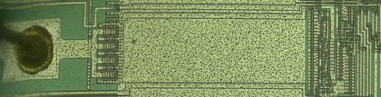
1) There are three types of ports present in the chip, which can be identified visually from the die images. The types are:
a) Input-only - one metal trace connected
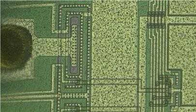
b) Output-only - two metal traces connected
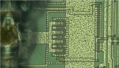
c) Bidirectional input/output - three metal traces connected
2) I catalogued the pins and made a list, which I then compared against the known connections from various Motronic schematics. The visual correlation of pin types matched the functional uses perfectly. Here is a listing of the pin numbers, the "labels" from the Bosch schematics and the port type.
Pin Label Type
1 ??? Out
2 CLK In
3 TV0/I10 In/Out
4 TV1/I11 In/Out
5 TV2/I12 In/Out
6 TV3/I13 In/Out
7 TV4 Out
8 PL Out
9 RESOUT Out
10 P2.7 In/Out
11 P2.6 In/Out
12 P2.5 Out
13 P2.4 Out
14 P2.3 Out
15 P2.2 Out
16 P2.1 Out
17 P2.0 Out
18 HST In
19 P1.0 Out
20 P1.1 Out
21 P1.2 Out
22 P1.3 Out
23 P1.4 Out
24 P1.5 Out
25 P1.6 Out
26 P1.7 Out
27 WUP Out
28 VTH In
29 I9 In
30 I8 In
31 I7 In
32 I6 In
33 I5 In
34 GND PWR
35 I5 In
36 I3 In
37 I2 In
38 I1 In
39 I0 In
40 RESET In
41 ??? Out
42 RD In
43 WR In
44 D0 In/Out
45 D1 In/Out
46 D2 In/Out
47 D3 In/Out
48 D4 In/Out
49 D5 In/Out
50 D6 In/Out
51 D7 In/Out
52 ALE In
53 A0 Out
54 A1 Out
55 A2 Out
56 A3 Out
57 A4 Out
58 A5 Out
59 A6 Out
60 A7 Out
61 PRG In
62 INST In
63 A13 In
64 A14 In
65 A15 In
66 CS0 Out
67 ??? Out
68 VCC PWR
3) Progress in understanding the control registers and command list is slow, but I have made a couple of small gains in this area. There are 6 controllable bidirectional pins (3, 4, 5, 6, 10, 11). The listing of the 13 commands sent from S700 to S702 at boot is shown below. You can see that there are 6 "small" low-byte addresses sent with a value of zero, which I am assuming is where those 6 pins are configured as outputs.
DPH DPL Data
A0 81 1
A0 10 81
A0 11 81
A0 40 FF
A0 41 FF
A0 2 0
A0 3 0
A0 4 0
A0 5 0
A0 8 0
A0 9 0
A0 21 D7
A0 20 FF
4) Pins 19-26 are listed as making up Port1 in the schematic. They are also output type pins, and immediately after FFh is sent to address A040h they toggle from low to high, so address A040h seems to be related to Port1. However, that same address is written to in other parts of the main loop and it does not toggle any Port1 pins, so there's more to it I assume.
5) Pin 66 looks to be configured as a buffer for A15, and it is used to toggle the RAM chip's enable pin. There is a possibility that the output of Pin 66 is a logical OR of A15 and A14 though...I need to confirm this with a small dummy program to mess with address lines.
6) Pin 67 appears to behave as another logical output. This one seems to be (A13 OR A14) OR (NOT A15). Again, I need to test this with a dummy program since A14 is never high when A15 is low as far as I can see in the stock ROM. My guess is that this is for an additional RAM/ROM/expander chip enable signal.
7) Pin 27 which is labeled as "WUP" in the schematic is not connected to anything in M1.7.3, but it is in M2.3.2. Despite this, it toggles between low/high every 10ms in my DME, immediately after S702 is written to (data FDh to address A040h). I do not observe any other outputs changing when this command is sent, so I have no clue as to why it is in the firmware to do this with an unused pin.
8) Eight other IO pins (the 6 bidirectional ones plus 12 & 13) change state after the 13th byte is sent during boot. However, their state transitions do not seem to correspond to any of the data bytes that were sent, so it may be that they are not accessed as "ports" in the same way that S700 and most microcontrollers do.
9) I assume that there is some sort of timer/counter onboard. Pin 2 is the "CLK" input, and I followed what I think is its trace through the die to an area with 6+ symmetric blocks of transistor logic. These may be the gate arrays which form the counter.
Again, high-res images of the S702 die are in the Dropbox.Leave a comment:
-
Thanks, I will look through those as well. I ruled-out the 8155/8255 family of devices a while back since they seem to be fairly different, but then again S702 might just be some sort of combination of the two.
I am doing edits on a local copy, but I can move the commenting over into the one on Dropbox.
Yeah HF...don't do a web image search for HF acid!Leave a comment:
-
HF acid.. Yeesh!
Did you edit the IDA project on dropbox, or did you copy a new one? I reccomend editing the live file - it better leverages everyone's input and expertise.Leave a comment:
-
Did Intersil mention this chip? I bet it's got some of the same logic in it:

Or could possibly be one of these :
Leave a comment:
-
Interesting. It is unlikely to be the same port expander, but there might be some useful info in there regarding the interface. Harris/Intersil made the part, and it was probably based on some existing expander out there. Intersil actually tried to help me find documentation for it, but it is so old that they did not have any that they could find, probably lost when Harris was spun off. My decapsulation and inspection of the silicon / metal layer helped me figure out which pins are inputs, outputs and bidirectional. Thus far I have not found any commercially available part with the same arrangement of IO's. Anyway, I have another thread on here where I RE'ed M1.7 and the S702 chip analysis is in there (some of it anyway). Since I have a pile of M1.7.x systems now, I am going to try to do a better RE job on the silicon now that I have better techniques, and there is a local chip-hacking community I found who may be helpful (I am not a fan of working with nitric or hydrofluoric acids in a DIY/home environment...I like to keep the bones that are in my fingers and functioning lungs).
Yeah, I figured out the jump tables...those seemed to be the one area that IDA was not able to trace properly since it is not emulating DPTR.
I mostly have a background writing assembly for PIC/dsPIC mixed signal systems, so there have been a couple of things to re-learn or change going to 8051 disassembly. Luckily, most of it is basically the same in terms of understanding the functionality. It's not my day job though, so I'm really more of a hobbyist when it comes to this stuff!Last edited by bmwman91; 03-20-2018, 01:49 PM.Leave a comment:
-
I had used a Motorola port expander with timers over 30 years back. Maybe the DME uses this part which I used.
I assume you understand how the jump tables work now - you posted about them 2 months back. If not, have a look here : https://books.google.ca/books?id=NHQ...age+jump+table
I've written loads of 8051 assembly language over the decades... I even wrote an interpreter that runs on a super fast 8051 core in a graphics chip when I worked at Genesis Microchip 20 years ago.Leave a comment:
-
Wow, NV-SRAM is fairly expensive! But, I guess it can save a lot of time. So that is one option anyway.
I am going through the disassembly now to start getting a better idea of it so that I can try to figure out S702. For now, I am basically starting from RESET and going through every single line and commenting it for myself so that I understand what is going on. I do not plan to do this for the entire code, but at least a thousand instructions or so to start getting a decent picture of the operation of some things (which in many cases involve S702 / DPTR = 0xA0xx).
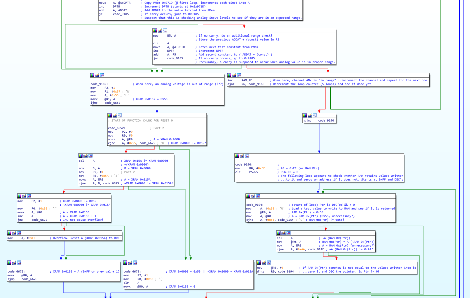
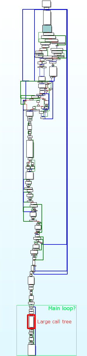
Looking at the IDA disassembly flow chart, the RESET code does various checks and then at the bottom of the flow ends up in a big sequence of LCALL instructions which seem to be table look-ups. This part at the end loops indefinitely it seems...is this the "main loop"?
Leave a comment:
-
Yes, I dont know why its decide use this thing with internal ROM. You can 0-0x1FFF area in EEPROM fill with 0xFF and all works fine :)
Just a little modify for original diagnostic communication code, work with NV-SRAM is simple - put WE pin to high and write to DPTR like in external RAM, put WE to low than work on. WE pin we has on PCB, and its represents to P55, so only simple DIP28 to DIP28 adapter is needed, and of course NV-SRAM programmer for first write. I have TLS866 PRO and it support write/read operations with NV-SRAM.Leave a comment:
-
I see, so S700 is likely an 80C515, not 535 in tat case?
I can work on how to adapt NV-SRAM to work here. I assume that you will have to rewrite the bootloader code which is in some "protected" address range, from which the rest of the addresses can have their data changed (sent from PC to K-line / UART, then into SRAM, then into NV-SRAM)?Leave a comment:
-
I'm check EEPROM write code today and unfortunatelly its write only to change coding bytes (as on all M1.1-M1.7.2) and can work only with UV-EPROM. Of course its possible to rewrite function to work with flash or nonvolatile SRAM. Last is preffered because there is possible to work without erase procedure, timings, specify around +13V constantly to DME for work... bmwman92 do you can make an PCB-adapter from EEPROM to NV-SRAM? We has averything needed on DIP socket, need just to change several pins.
Also I'm notice that EA pin is connected to 5V, so checked firmware with empty 0-0x1FFF and give worked ECU :) So first 0x2000 bytes is also used from CPU and equal M1.7.2.Leave a comment:
-
It was a question of if you could get a useful RAM dump. If the answer is no, that's OK. It's not necessary but it can be helpful.
Although I think you misunderstand me (again). When I say "not a running car" I mean the DME has to be booted up and running on a bench, or obviously the contents of RAM would be useless.Leave a comment:
-
WOT table in M1.7.3 is not table in Motronic terms, but just data array which value given from "mov a, @A+DPTR", where A = -(RPM-CONST)
I'm not say that is impossible to change WOT table, but only with recompilation like FGAT functional which I'm added in custom software.
Maybe for temporary fast edited tables in RAM or just for stock or just because cost 8k x 8/4k x 8/2k x 8 (minimum value for all Motronics) is almost equal or because hardware is done by one team and software by another and who knows how RAM is needed in new software and the alteration of PCB and documentation is too high price then? Anyway its good, because we can use extra memory as we need.
Because you take these words literally :) After reset 80C515 fill his internal RAM with 0xFF, external memory permanently connected to power (+12, if we say in car terminology, not in electronics) and hold previously saved values, but if we reconnect +12 to ECU, external ram will be reset and filled with garbage values. Some values in external ram is filled after reset 80C515, but whole external ram is not filled with 0xFF, its impermissiblely long time and does not any sense. Understand what I mean? And why I say than nando aspirations does not any sense.Also, I am not understanding the comment about external memory being connected to +12...I did not see anything like that when I was building the schematic.Last edited by Rasp; 03-17-2018, 12:00 AM.Leave a comment:


Leave a comment: